Experimental physicist · Quantum devices

Mohammad Javadi BalakanMJ Balakan

I'm an experimental physicist exploring quantum matter by engineering nanoscale devices. My research focuses on topological superconductivity, a promising route to quantum computers that are naturally protected from errors. Over more than a decade, I've turned new materials into working technologies, from CMOS-compatible 2D-material devices to superconducting circuits with exotic quantum properties. I'm now combining this experience with AI to develop actionable knowledge.

Most recently Research Scientist at SUNY Albany (CNSE); previously at the University of Tehran.

Φ₀ = h/2e ≈ 2.068 × 10⁻¹⁵ Wb

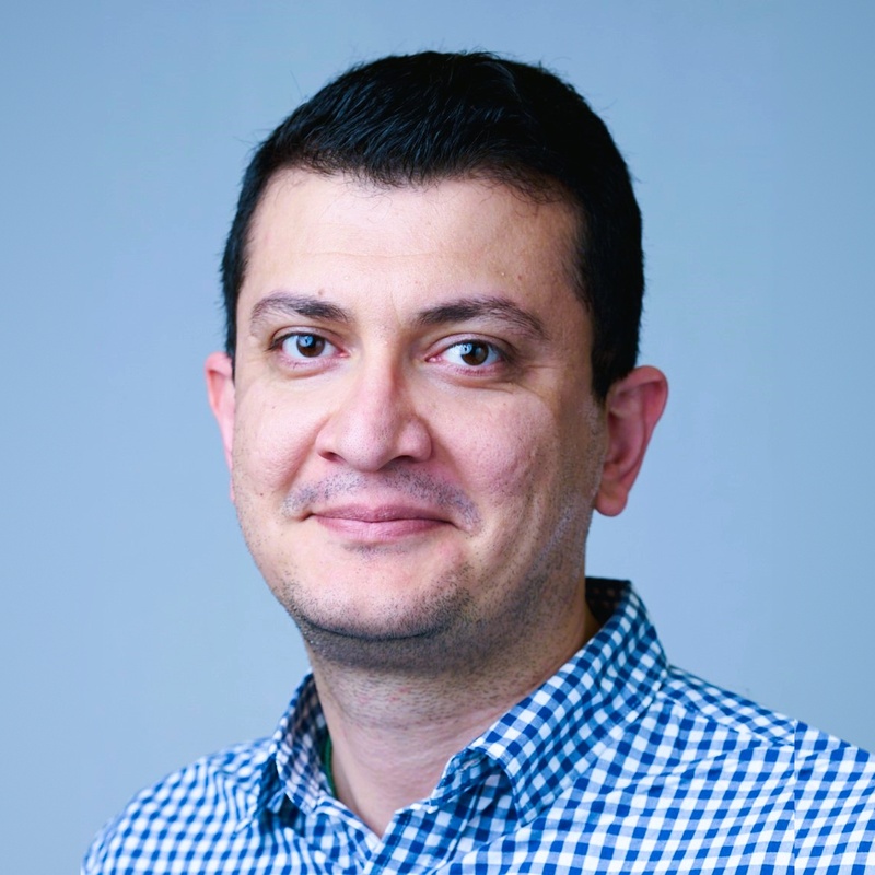
Portrait of Mohammad Javadi Balakan
Research · 2022 – 2026

Topological
superconductivity
for quantum
computing

Topological superconductors combine the quantum coherence of a superconductor with the protection of topology. They can host Majorana modes, the building blocks of qubits that are far less prone to errors. Proving that a material is a topological superconductor is hard, because its exotic states are hidden beneath a superconducting bulk. The iron-based superconductor Fe(Te,⁠Se) is one of the most promising candidates. We fabricate fully encapsulated ring devices, a few hundred nanometers across, and probe them with low-noise, phase-sensitive measurements at a few kelvin. A ring architecture forces the superconducting wavefunction to wind around a closed loop, leading to flux quantization inside the ring. Such quantization can reveal the condensate's topological phase, its complex spin texture, and other associated exotic properties.

2014 – 2021 · University of Tehran

Earlier: 2D materials and silicon devices

Before quantum devices, I worked on bringing new materials into silicon technology for light sensors, solar cells and future chips, combining device experiments with physical modeling.

2018 – 2021

CMOS-compatible devices from 2D materials

Graphene lets light pass into the silicon beneath it, which makes graphene–silicon junctions attractive for solar cells and detectors. We showed that charge crossing this 2D/3D interface is limited by how slowly electrons leave the graphene plane, and calculated the efficiency limit of graphene–silicon solar cells. We also grew borophene, a one-atom-thick metal, by chemical vapor deposition, a scalable route to 2D interconnects.

2017 – 2020

Hybrid organic–silicon optoelectronics

Coating silicon with a conductive polymer gives junctions that are made at low temperature from solution and work over large areas. We worked out how charge moves through them, injection over an interface barrier in one direction and space-charge-limited flow through the polymer in the other. On this platform we built position-sensitive detectors and self-powered photodiodes that stay stable after long exposure to air.

2014 – 2018

Solar cells and physical modeling

Our Monte Carlo simulations showed that confining a porous oxide network steers electrons toward the collecting electrode. We then built column-structured dye-sensitized solar cells and measured longer electron lifetimes and diffusion lengths. With COMSOL and numerical models, we also explained how plasma-enhanced CVD produces self-organized, single-standing carbon nanotubes.

Recognition & news

Recent

Publications

Selected papers

Each title opens a one-page summary with the key result, figure and links.

All papers and preprints
Experience

Career & education

  • 2025–26Research ScientistCNSE, SUNY Albany · group of Prof. Ji Ung Lee
  • 2022–24Postdoctoral FellowCNSE, SUNY Albany · topological superconductors for fault-tolerant quantum computation
  • 2019–21Postdoctoral AssociateDepartment of Physics, University of Tehran · CMOS-compatible devices from 2D materials
  • 2018Visiting ResearcherPhysics, Sapienza University of Rome ·
    Prof. Giorgio Parisi, 2021 Nobel Laureate in Physics
  • 2019PhD, Solid-State PhysicsUniversity of Tehran
  • 2014MSc, Nanoscience and NanotechnologyUniversity of Tehran
  • 2012BSc, PhysicsUrmia University
Honors
  • Chamran Postdoctoral Fellowship · Iran National Elites Foundation (INEF), 2020
  • Outstanding PhD Thesis in Physics (nationwide) · Physical Society of Iran, 2019
  • Outstanding PhD Dissertation in Physical Sciences · University of Tehran, 2019
  • INEF Graduate Scholarship · 2016 - 2018

Reviewer for Physical Review Letters, 2D Materials, Applied Physics Letters, Nanotechnology

Toolkit

Hands-on skills

Fabrication
Cleanroom nanofabricationElectron-beam lithographyFocused ion beamReactive ion etchinghBN encapsulationPVD and e-beam evaporationCVD and PECVD
Measurement
Cryogenic quantum transportLock-in and low-noise measurementCryogenic filter designPhase-sensitive flux measurementSEMAFMRaman spectroscopyOptoelectronic testing
Computation
PythonInstrument automationLabVIEWMathematicaKLayout mask designMonte Carlo and COMSOL modeling
Contact

Get in touch

For research collaborations, talks, or roles in quantum and semiconductor device development.

Profiles